Triple-Junction GaAs Solar Cell — Structure and Gains
Table of Contents
Quick answer: A triple-junction GaAs solar cell stacks three photovoltaic junctions, each tuned to absorb a different band of the solar spectrum, on a gallium arsenide substrate. Because each junction converts only the photons it is matched to, and the unused light passes through to the layer below, the stack converts far more of the spectrum than a single-junction silicon cell. This is why triple-junction GaAs cells exceed 30% efficiency under concentration, against roughly 22% to 24% for mainstream silicon. The trade-off is cost: GaAs epitaxy on germanium or GaAs substrates is orders of magnitude more expensive per watt than silicon, so the technology is confined to concentrator photovoltaics and spacecraft, where power per kilogram matters more than cost per watt. Space arrays use them because mass and stowed area are the limiting constraints.
PV Module Manufacturing · by Jerry, Ooitech
Introduction
As commercial spaceflight keeps growing, spacecraft need more and more electrical power. Space photovoltaics serve as the main power source for most spacecraft, so the choice of solar cell technology directly shapes whether a mission succeeds, how cost-effective it is, and how competitive it stays in the market.
Right now, there are three main technology directions: gallium arsenide (GaAs), p-type heterojunction (HJT), and p-type HJT/perovskite tandem cells. Looking at where the technology is heading and its long-term potential, and digging into the core pros and cons of each route, GaAs still comes out on top. Despite the cost challenges, its unmatched all-around performance, proven reliability in extreme environments, and clear, sizable room for cost reduction make GaAs the best pick for high-value, high-reliability commercial space missions both today and over the next 3-5 years.
The Advantages of Triple-Junction GaAs Cells
High efficiency
The GaAs bandgap (1.42 eV) sits right in the theoretically optimal range. On top of that, multi-junction cells stack GaInP, GaAs, and Ge layers that absorb high-, medium-, and low-energy photons respectively, which greatly widens the spectrum they can use. The latest triple-junction GaAs cells for space photovoltaics now reach power conversion efficiencies above 30%.
High reliability
Strong radiation resistance and excellent high-temperature stability make these cells a perfect fit for the core needs of high-end, long-life missions. The performance edge is enough to offset the higher cost.
Mature technology with a long track record in orbit
Back in 1965, the former Soviet Union's Venera 3 satellite became the first to use GaAs cells. In 1995, the first commercial communications satellite MEASAT used single-junction GaAs as its main power unit, and the solar array design built up a complete database proving that GaAs cells could meet a spacecraft's full life-cycle power needs. From then on, GaAs cells gradually replaced older cells as the basic power-generating unit on spacecraft, evolving step by step from single-junction to multi-junction designs.
Why Design It as a Three-Junction Structure?
Any semiconductor material can only efficiently absorb photons with energy greater than its bandgap. Photons with too little energy can't be used, while photons with too much energy lose the excess as heat (thermalization loss). A single-junction cell's bandgap can't perfectly match the solar spectrum. Take a single-junction silicon cell as an example: it can absorb photons in the 0.3-1.1 μm range (300 nm-1100 nm), mainly working in the 0.38 μm-0.7 μm band. That's why single-junction silicon cells have a limited efficiency ceiling, with a theoretical limit of around 29.7%.
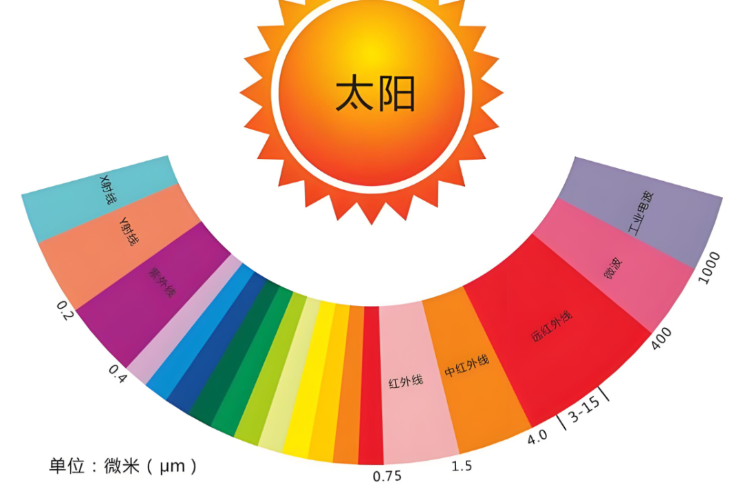
A three-junction cell splits the work across three sub-cells, slicing the solar spectrum into three segments so each sub-cell operates in its best-suited band. This sharply cuts both thermalization losses and spectral mismatch losses. In theory, multi-junction cells can approach 50% efficiency, far higher than what a single-junction structure can deliver.
The Structure of a Triple-Junction GaAs Cell
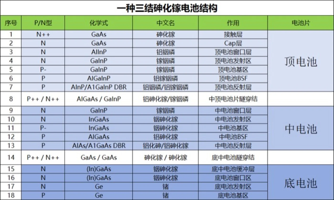
The triple-junction GaAs cell is divided into three parts: the top cell, the middle cell, and the bottom cell. Each part uses different main (base region) materials and plays a different role.
Top cell
Usually AlGaInP / GaInP, with a bandgap around 1.8-1.9 eV. It mainly absorbs short-wavelength photons (ultraviolet, blue light). The top cell soaks up high-energy photons and reduces thermalization losses.
Middle cell
Usually InGaAs or GaAs, with a bandgap around 1.42 eV. It mainly absorbs medium- and long-wavelength photons (green, yellow, red light). The middle cell handles the medium-to-long wavelengths and contributes most of the photocurrent.
Bottom cell
Usually Ge, with a bandgap around 0.67 eV. It mainly absorbs long-wavelength photons (near-infrared). The bottom cell captures the highly penetrating infrared light.
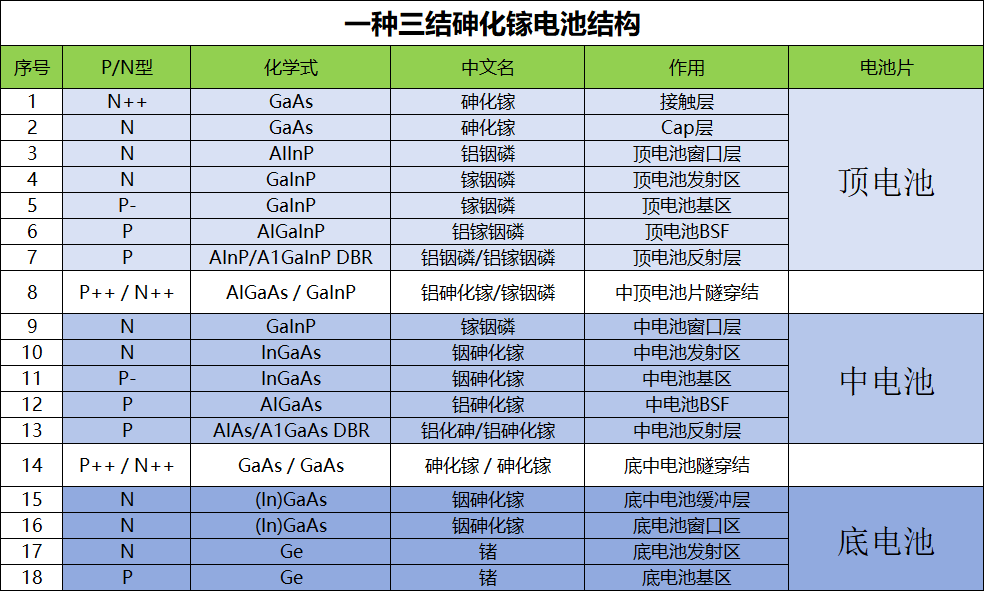
Now let's walk through what each layer does.
① Contact Layer
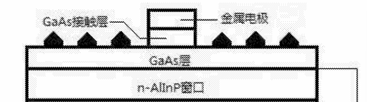
Sitting right above the outermost Cap layer, this is the semiconductor layer that the metal electrode directly touches. It is usually heavily doped n⁺⁺-GaAs or n⁺⁺-GaInP. Its main job is to lower the contact resistance—heavy doping helps it form a good ohmic contact with the metal electrode and cuts down on electrical losses. It also protects the active region, isolating the metal electrode from the delicate active region below (window layer, emitter, etc.) to prevent process damage.
② Cap Layer
Located above the window layer and below the anti-reflection coating, sitting between the anti-reflection film and the contact layer. It is commonly GaAs, though some designs use transparent conductive oxides (TCO) such as ITO. Its main role is to assist current collection as an "auxiliary electrode," working with the contact layer to gather and lead out current laterally—especially useful for fine-line grid designs. Its thickness and refractive index can also be tuned to take part in optical design and provide an auxiliary anti-reflection effect.
③ Window Layer
Located above the emitter, usually made of AlInP, AlGaInP, or AlGaAs. Its main role is to reduce surface recombination: the material's wide-bandgap nature means it absorbs little light, and it forms a high-low junction that pushes photo-generated carriers (electrons) toward the interior of the emitter, cutting recombination losses at surface defects. It also acts as an "umbrella," protecting the junction region from damage during later processes such as electrode evaporation.
④ Emitter
Located below the window layer and above the base, forming a PN junction with the base. It is usually N-type GaInP or GaAs. Its main role is to act as the "positive electrode," collecting photo-generated electrons and conducting them to the external circuit. It also balances light absorption against collection—through careful tuning of thickness and doping concentration, it is thick enough to absorb short-wavelength light but not so thick that carriers recombine during diffusion.
⑤ Base
Located below the emitter and above the BSF layer, this is the main body of the PN junction. It is usually p-type GaInP or AlGaInP. As the main light-absorbing region, it is the "workhorse" of the top cell, absorbing most of the short-wavelength light (blue and ultraviolet), generating photo-generated electron-hole pairs, and efficiently transporting the photo-generated holes to the back BSF layer or electrode.
⑥ BSF Layer (Back Surface Field)
Located below the base and above the tunnel junction, forming a high-low junction with the base on the back side. The material is usually a wide-bandgap p-AlGaInP, AlGaAs, and the like. Its main role is to suppress reverse carrier recombination: the BSF layer creates a "barrier" on the back of the base that stops photo-generated holes from being recombined as they diffuse toward the back electrode, thereby boosting voltage and efficiency.
⑦ Reflector
Located between the top cell and the middle cell, or between the middle cell and the bottom cell. It is a Distributed Bragg Reflector (DBR) grown from alternating high- and low-refractive-index materials, such as AlAs/AlGaAs or AlInP/AlGaInP. Its main job is to reflect back the medium-to-long-wavelength light that the top and middle cells haven't absorbed and is about to escape, allowing for a second absorption pass that lifts overall current and efficiency.
⑧ Tunnel Junction
Located between the sub-cells, made of heavily doped thin layers (such as n++GaAs / p++GaAs). Like a "quantum tunnel," it lets photo-generated carriers pass through efficiently while keeping each sub-cell electrically independent.
The middle cell's structure is similar to the top cell's, just with different materials, so we won't repeat it here. Below we briefly cover what's different about the bottom cell.
⑨ Buffer Layer
Sandwiched between the bottom cell and the middle cell, it solves the lattice-mismatch problem. When the bottom cell material (such as InGaAs) doesn't match the lattice constant of the upper material (such as GaAs), the buffer layer uses a "graded" or "metamorphic lattice" structure to gradually release stress and "intercept" threading dislocations, keeping them out of the bottom cell's active region and thereby improving cell performance.
⑩ Bottom Cell Base
Located on the "thick" side of the bottom cell's PN junction. It is usually a p-type Ge substrate. Its main function is to absorb long-wavelength infrared light, serving as the workhorse for generating photo-generated carriers in the bottom cell.
A Few Notes
In the P/N type labels, N++/P++ and similar markings indicate light versus heavy doping. The triple-junction GaAs cell structure illustrated in this article omits the electrode structure, anti-reflection layer structure, and similar details for simplicity.
References:
Triple-junction solar cell with a reflector and its fabrication method - 2022-0804
InGaP/InGaAs/Ge triple-junction solar cell with a micro-nano anti-reflection structure and its fabrication method - 2018-0425
A method for a triple-junction solar cell and the triple-junction solar cell - 2020-11-13
Ooitech's View
Ooitech believes: triple-junction GaAs cells, by slicing the solar spectrum across three sub-cells, deliver the high efficiency and proven reliability that make them the leading choice for today's high-value space power missions.