TBC Solar Cell Technology (TOPCon Back Contact): Full Process Guide
Table of Contents
Technology Overview
The content below is shared for reference only. If there is any technical infringement or incorrect guidance, feel free to contact the author for removal or correction.
What is a TBC cell?
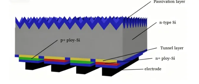
TBC stands for TOPCon Back Contact. It fuses TOPCon passivation (tunnel oxide plus poly-silicon) with the IBC interdigitated back contact structure, so people also call it a POLO-IBC cell.
It deep-integrates the TOPCon tunnel oxide / poly-Si passivation with the IBC back contact layout. That gives you the strong rear passivation of TOPCon plus the IBC advantage of no front gridline shading, with all current collection moved to the back. The result is higher open-circuit voltage and higher short-circuit current. It's one of the mainstream N-type high-efficiency routes for the next generation.
Core advantages
No front metal gridlines, so front shading loss is removed and Isc goes up
TOPCon tunnel passivation lowers rear recombination and lifts Voc
The interdigitated P/N back contact layout optimizes the carrier collection path and cuts series resistance
Compared with standard TOPCon and standard IBC, it balances passivation quality and structural integration
Compatible with most core equipment on existing N-type lines, so the process can be upgraded step by step
How it compares with conventional cells
Standard TOPCon: front gridline shading, full-area TOPCon passivation on the rear
Standard IBC: back contact structure, but passivation relies on silicon oxide / silicon nitride, no tunnel poly-Si passivation
TBC (POLO-IBC): IBC back contact structure plus integrated TOPCon tunnel passivation, so both structure and passivation are optimized
Full Process Flow Overview
Wafer incoming → pre-cleaning / saw damage removal → rear tunnel oxide + poly-Si deposition (LPCVD) → rear SiN mask deposition → first rear laser opening (boron area) → boron doping (p-poly) → second rear laser opening (phosphorus area) → phosphorus doping (n-poly) → cleaning to strip wrap-around diffusion / BSG / PSG → rear passivation film deposition → wax mask printing to protect the rear → front texturing + P/N isolation etch → front and rear SiN anti-reflection passivation film deposition → rear metal electrode screen printing → firing → electrical test → sorting and packing
Detailed Process Specifications
3.1 Cleaning and polishing (pre-clean + saw damage removal)
Purpose: remove the saw damage layer, surface metal impurities, particles and oil; polish the wafer single or double sided to get a clean, flat silicon base and keep the later tunnel layer deposition uniform.
Main equipment: inline wet cleaning and polishing line, alkaline polishing tank, acid cleaning tank.
Key chemicals: strong alkali (NaOH/KOH), HF, HCl, IPA, texturing additive, surfactant.
Key monitoring items:
Polishing weight loss: electronic balance
Surface reflectance: reflectance tester
Minority carrier lifetime iVoc: WCT-120 transient lifetime tester
Carrier recombination imaging: PL tester (R3-PL)
Surface roughness and cleanliness: optical microscope
Quality control: saw damage fully removed, no stains or steps on the surface, uniform weight loss, no obvious lifetime drop.
3.2 Tunnel oxide + poly-Si deposition
Purpose: grow an ultra-thin tunnel oxide (SiO₂) then an intrinsic poly-Si layer on the wafer rear, forming the core TOPCon passivation structure for strong field and chemical passivation and low rear recombination.
Main equipment: tube LPCVD.
Gas sources: SiH₄, O₂, N₂ (carrier / purge).
Key items:
Poly-Si thickness: poly thickness tester, ellipsometer
Tunnel oxide thickness: ECV, ellipsometer
iVoc (WCT-120)
PL uniformity
Sheet resistance (intrinsic poly monitoring before doping)
Quality control: oxide ultra-thin and uniform, poly-Si dense and pinhole-free, good thickness consistency across the wafer.
3.3 Rear SiN mask deposition
Purpose: deposit a dense silicon nitride (SiNₓ) layer on the intrinsic poly-Si as a blocking mask for the later laser opening and doping steps, enabling selective doping zones.
Main equipment: PECVD.
Gas sources: SiH₄, NH₃, N₂.
Key items: SiN thickness (spectroscopic ellipsometer), refractive index and uniformity, iVoc, PL uniformity.
Quality control: dense mask, no pinholes, uniform thickness to guarantee doping isolation.
3.4 First rear laser opening (boron diffusion window)
Purpose: selectively remove the SiN mask over the boron diffusion area by local laser ablation while keeping the intrinsic poly-Si underneath, opening the window for the later p-type poly.
Main equipment: fiber / nanosecond or picosecond laser opening system, high-precision laser patterning tool.
Process tuning: adjust laser power, repetition rate, scan speed and spot overlap so only the top SiN mask is removed and the intrinsic poly-Si below is not damaged, keeping the passivation base intact.
Key characterization: optical microscope check of groove shape, edge integrity, and whether the poly layer is burned.
3.5 Rear boron doping (p-poly)
Purpose: boron-diffuse the intrinsic poly-Si in the opened area to convert it into p-type heavily doped poly (p-poly), while forming BSG on the surface. The BSG later acts as a natural blocking mask for phosphorus diffusion.
Main equipment: tube boron diffusion furnace.
Process media: liquid source BBr₃; ambient O₂, N₂.
Key characterization: p-zone sheet resistance, doping uniformity, BSG coverage integrity, PL doping uniformity.
Quality control: sufficient boron doping, uniform sheet resistance, continuous and complete BSG with no local gaps.
3.6 Second rear laser opening (phosphorus diffusion window)
Purpose: remove the remaining SiN mask to expose the undoped intrinsic poly-Si as the n-type phosphorus doping zone, while keeping the already formed BSG layer intact from laser damage.
Main equipment: laser patterning / opening system.
Process focus: precise laser energy control to avoid punching through the BSG layer, keeping a clean isolation boundary between P and N zones.
3.7 Rear phosphorus doping (n-poly)
Purpose: phosphorus-diffuse the second-window intrinsic poly-Si to form n-type heavily doped poly (n-poly). The BSG formed in the previous step works as a self-aligned mask, blocking phosphorus from diffusing into the p-poly area and achieving self-isolation of the P/N zones.
Main equipment: tube phosphorus diffusion furnace.
Process media: liquid source POCl₃; ambient O₂, N₂.
Key principle: the residual BSG acts as a natural diffusion barrier and stops phosphorus contamination of the p-poly area. After phosphorus diffusion the BSG partly turns into a boron-phosphorus mixed oxide, which further strengthens the isolation.
Key characterization: n-zone sheet resistance, P/N boundary isolation, leakage trend monitoring.
3.8 Cleaning to strip wrap-around diffusion (BSG/PSG removal)
Purpose: chemically remove all BSG, PSG and surface residues, and strip the edge wrap-around and side doping layers to avoid edge leakage.
Main equipment: inline wet cleaning line.
Key chemicals: mainly HF, plus acidic additives and a buffered acid system.
Process aids: clean dry air blow-off, hot air drying.
Quality control: oxide glass fully removed, clean surface with no residue, no wrap-around residue at the edges.
3.9 Rear SiN passivation protective film deposition
Purpose: deposit a SiN passivation protective film on the rear interdigitated P/N poly structure to passivate and protect the back contact area and block chemical attack in later steps.
Main equipment: PECVD.
Gas sources: SiH₄, NH₃, N₂.
Characterization: SiN thickness, refractive index, film uniformity.
3.10 Rear wax mask coating (protective mask)
Purpose: fully coat the rear with a wax protective layer by screen printing to shield the formed P/N back contact structure and SiN film, preventing the later front etch from attacking the rear functional layers.
Main equipment: screen printer (wax printing station).
Control focus: complete wax printing, no skip printing, no pinholes, good edge sealing so the rear stays protected throughout.
3.11 Front chemical etching + wax stripping and cleaning
Purpose:
Remove excess doping and damage layers on the wafer front
Texture the front to form a pyramid surface and cut front reflection
Achieve edge isolation between the rear P and N zones through lateral etching to reduce edge leakage
Finally strip the rear wax mask to expose the complete back contact structure
Main equipment: double-sided inline wet etching and texturing line.
Key chemicals: strong alkali (NaOH), HF, texturing additive, buffered etchant.
Gas sources: clean compressed air, N₂ blow-off.
Quality control: uniform front texturing, qualified pyramid morphology, proper P/N isolation, no leakage path, clean wax stripping with no residue.
3.12 Front and rear SiN anti-reflection passivation film
Purpose: deposit a SiN anti-reflection passivation film on the front for both anti-reflection and surface passivation; add and optimize the rear passivation film to further improve passivation and reliability.
Main equipment: PECVD.
Gas sources: SiH₄, NH₃, N₂.
Characterization: front and rear film thickness, refractive index, minority carrier lifetime, reflectance.
3.13 Rear electrode screen printing and firing
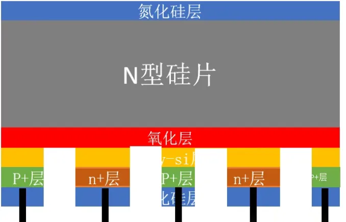
Purpose: print silver-aluminum electrodes on the rear P zone and silver electrodes on the n-type poly zone to form the interdigitated back contact positive and negative electrodes, then use high-temperature firing to form ohmic contact between the metal and the doped poly-Si.
Main equipment: dedicated back contact screen printer, inline firing furnace.
Key steps: rear electrode pattern alignment printing → drying → high-temperature firing (forming ohmic contact).
3.14 Back-end inspection and sorting
Process content: EL inspection (defects, micro-cracks, leakage), IV electrical test (Voc, Isc, FF, Eff), appearance inspection, grading and sorting, packing and warehousing.
Inspection equipment: EL tester, IV tester, appearance inspection station.
Key Challenges and What to Focus On
What are the tough parts of TBC technology, and where should attention go?
Controlling the thickness uniformity of the ultra-thin tunnel oxide is hard
The two laser opening steps demand extremely high alignment accuracy
Keeping the BSG self-aligned mask intact is the core of the process
The P/N interdigitated isolation etch is prone to edge leakage
Back contact electrode printing needs higher alignment accuracy than conventional cells
Managing minority carrier lifetime decay across the whole flow is difficult
Key SPC parameters to watch
Tunnel oxide thickness and poly-Si thickness
Laser opening morphology and alignment deviation for both steps
Sheet resistance uniformity of boron and phosphorus diffusion
iVoc and PL minority carrier lifetime tracked across the whole flow
Front reflectance and texturing morphology
EL micro-cracks, leakage, and edge isolation status
Ooitech's View
TBC lives or dies on the details, and the BSG self-aligned mask is the quiet hero here since it lets phosphorus and boron zones sort themselves out without a third mask step. What we watch most on module lines is how these high-Voc back contact cells behave downstream in stringing and lamination, because their all-rear metallization changes the interconnection game. If you want to see real N-type module lines running, our YouTube channel www.youtube.com/ooitech has factory footage worth a look.